Sep 2026· IEEE Journal of Solid-State Circuits· Vol 61, pp. 5098-5110· 0 citations· 35 references
Abstract
Static random-access memory (SRAM)-based computing-in-memory (CIM) macros have been widely studied to improve the energy efficiency of edge artificial intelligence (AI) inference tasks. However, less attention has been given to AI training, which requires CIM macros to not only perform matrix multiply-accumulate (MAC) operations but also support matrix transposition. To address the limitations of previous analog transpose and digital non-transpose SRAM CIM macros, this work features: 1) a cyclic-weight-mapping SRAM array that enables matrix transposition and reuse of MAC circuits during both feed-forward (FF) and back-propagation (BP) phases; 2) a digital CIM architecture employing signed fixed-point mantissa encode and a vector-wise pre-alignment (VWPA) scheme, supporting multiple data formats including INT4/8, FP8, and BF16; and 3) an accurate/approximate dual-mode bit-parallel MAC circuit (DMBP-MAC) designed to provide a tradeoff between computational accuracy and energy efficiency. A fabricated 28-nm 32-kB transpose SRAM CIM macro achieved average energy efficiency of 70.2–285.4 TOPS/W in INT4, 17.5–71.4 TOPS/W in INT8, 51.1–192.3 TFLOPS/W in FP8, and 12.8–48 TFLOPS/W in BF16.
SRAM-based compute-in-memory (CiM) accelerators have emerged as a promising approach for low-power inference in edge devices by alleviating data-movement overhead. However, existing CiM designs face a fundamental trade-off: integer-based CiM suffers from limited numerical accuracy, while floating-point CiM incurs substantial energy and area overhead due to complex exponent handling and peripheral circuits. This paper presents an analog CiM accelerator based on the SMX6 format, which extends the block floating-point (BFP) representation with a lightweight microexponent (μE) shared by pairs of values. By embedding μE-aware scaling directly into the analog MAC operation, the proposed design achieves improved numerical fidelity without introducing costly digital shift-and-align logic. To further address accuracy degradation caused by analog dynamic-range limitations, the accelerator supports configurable block granularity, allowing the accumulation range to be adaptively adjusted to match layer-wise activation distributions and ADC input constraints. Implemented in 28nm CMOS technology, the proposed SRAM-based ACiM achieves accuracy close to the FP32 baseline across diverse workloads, while delivering up to 54.19 TOPS/W energy efficiency and 4.66 TOPS/mm2 area efficiency. These results demonstrate that micro-exponent-aware analog CiM with configurable granularity is an effective and practical design point for energy-efficient edge inference.
W. Han, Dohyun Kim, Jihoon Park et al.· Proceedings of the ACM/IEEE...· 0 citations
Digital computing-in-memory (DCIM) provides deterministic floating-point computation but incurs substantial area and power overhead from replicated mantissa multipliers and adder trees. This work proposes an error-recoverable BF16 DCIM arithmetic unit that jointly approximates a 2-bit multiplier and the first adder stage. For the 11 × 11 input, the multiplier outputs 0111 instead of the Baseline 1111, converting the error from +6 to −2 and fixing the product MSB to 0. This enables the first adder stage to be reduced from 4 bits to 3 bits. A lightweight flag detects the same error condition and is reused as a carry input for local compensation, avoiding a separate multi-bit correction circuit. Hierarchical design-space exploration selected the 0111 approximation with carry compensation at bit position 1. Transistor-level evaluation showed reductions of 14.81% in transistor count and 28.56% in average power relative to the Baseline. Across ResNet18, VGG16-BN, and AlexNet on CIFAR-10 and CIFAR-100, the Proposed scheme achieved the lowest BF16-referenced Layer NRMSE and Logit NRMSE among the evaluated Baseline, DIMC-S-derived, LSAC OR+SXAFA-derived, and Proposed schemes, while the Top-1 accuracy difference relative to the Baseline remained within −0.02%p to +0.12%p. These results demonstrate an improved hardware–accuracy trade-off without retraining or data rearrangement.
Adder neural networks remove multiplication from convolution, yet their direct L1-distance datapath still requires subtraction, absolute-value generation, and wide accumulation. We address this cost by mapping the online L1 operation to minimum selection and time-domain accumulation. The proposed accelerator processes a 3×3×16 window for 16 output channels with 6-bit weights and activations. Each 6-bit minimum is divided into two 3-bit slices. A dual-mode digital-to-time converter (DM-DTC) encodes the most-significant slice in high-linearity (HL) mode and the least-significant slice in low-power (LP) mode. Readout is performed by a shared-clock time-to-digital converter (SC-TDC), in which one Gray-code time reference serves all paths while local latches preserve independent channel results. The training model reproduces code-dependent DTC nonlinearity, process–voltage–temperature variation, jitter, channel offset, TDC quantization, saturation, and scale mismatch. The architecture thereby combines significance-aware time encoding, channel-scalable readout, and hardware-aware adaptation. Post-layout simulations in 55 nm show that the 0.359 mm2, 13.7 Kb design operates at 0.7–1.2 V and 5–30 MHz, consumes 0.025–0.324 mW, and achieves 43.2–94.3 TOPS/W. The normalized figure of merit is 6.01–13.09 POPS/W·bit2. On CIFAR-10/ResNet-20, hardware errors reduce the baseline accuracy from 92.71% to 86.26%; error-aware training achieves 91.53%.
Aoming Zhan, Ye Zhao, Yumei Zhou et al.· Applied Sciences· 0 citations
Compute-in-Memory (CIM) based on resistive random access memory (RRAM) offers significant advantages in energy efficiency and parallelism, making it a promising solution for accelerating neural networks. However, the computational accuracy, energy efficiency, and flexibility of current CIM chips are still challenged by practical issues such as device and circuit-level non-ideality and the high overhead of peripheral circuits, which remain inadequately addressed in existing designs. To address these challenges, this work proposes REF-CIM, a 40nm robust, energy efficient and flexible RRAM- CIM macro that achieves non-ideality tolerance, high energy efficiency and configurable precision, featuring: 1) a complementary multi-bit input unit (CMIU) with symmetric bit-line access; 2) a proportional current-scaling clamp circuit (PCSC); 3) a distributed tree-based sparse analog-to-digital converter (DTS-ADC); and 4) a configurable multi-mode deployment scheme for supporting diverse neural network precisions. The performance of the proposed macro is evaluated through chip measurements, considering non-ideal effects such as IR-drop, device variation, and analog circuit noise. Simulation results calibrated with measurement data demonstrate a peak energy efficiency of 29.1 TOPS/W@8bIN/8bW/16bOUT, with classification accuracy reaching 92% on the CIFAR-10 dataset under 10% device variation.
H. Ding, Yunfan Yang, Zongwei Wang et al.· IEEE Transactions on Circuit...· 0 citations
The traditional von Neumann architecture faces a severe memory wall bottleneck in modern data-intensive artificial intelligence applications. Memristor-based Computing-in-Memory (CIM) is a promising approach to reduce data movement, but conventional analog CIM remains vulnerable to read noise, sneak path currents, device variation, and the area and power overhead of high-resolution Analog-to-Digital Converters (ADCs). This work presents a schematic-level digital near-memory computing architecture based on a 1-Transistor-3-Resistor (1T3R) bit-slicing scheme for 3-bit signed weight storage. Each weight is mapped to three binary memristor states using two's complement representation, and the sensed digital outputs are processed by a low-bit pipelined Multiply-Accumulate (MAC) and Rectified Linear Unit (ReLU) backend. This design avoids high-resolution analog current readout and shifts the main computation to compact digital logic. The memristor array, write-inhibit and read control scheme, and digital processing blocks are implemented and functionally verified at schematic-level in Cadence Virtuoso using the open-source SkyWater 130 nm Process Design Kit (PDK) at a nominal 1.8 V supply. For system evaluation, a Python simulation framework is developed to incorporate the same low-bit quantization, signed weight mapping, finite bit digital arithmetic, and modeled device nonidealities. Hardware-aware simulations on Modified National Institute of Standards and Technology (MNIST) indicate that the proposed architecture can maintain functional classification capability under 3-bit weight and 2-bit input constraints. The reported macro power, performance, and area values are first-order projections from schematic simulations and scaling assumptions. Layout implementation, parasitic extraction, and post-layout validation remain future work.
Zeyuan Hou, Xiaomeng Wang, Yang Yi· Journal of Electronics and E...· 0 citations
Related blog posts
MIT News · Artificial Intelligence· news.mit.eduSep 2, 2026
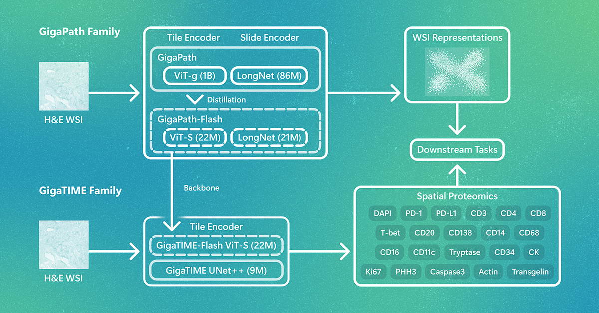
What if pathology foundation models could do more with less? GigaPath-Flash and GigaTIME-Flash cut computational demands while maintaining strong performance, opening the door to larger studies and broader exploration. The post GigaPath-Flash and GigaTIME-Flash: Toward population-scale discovery with efficient pathology foundation models appeared first on Microsoft Research.
MIT News · Artificial Intelligence· news.mit.eduAug 31, 2026
With millions of users across the world, Julia has been used to conduct cutting-edge research and to design new drugs, jet engines, heat pumps, and more.
MIT News · Artificial Intelligence· news.mit.eduAug 27, 2026
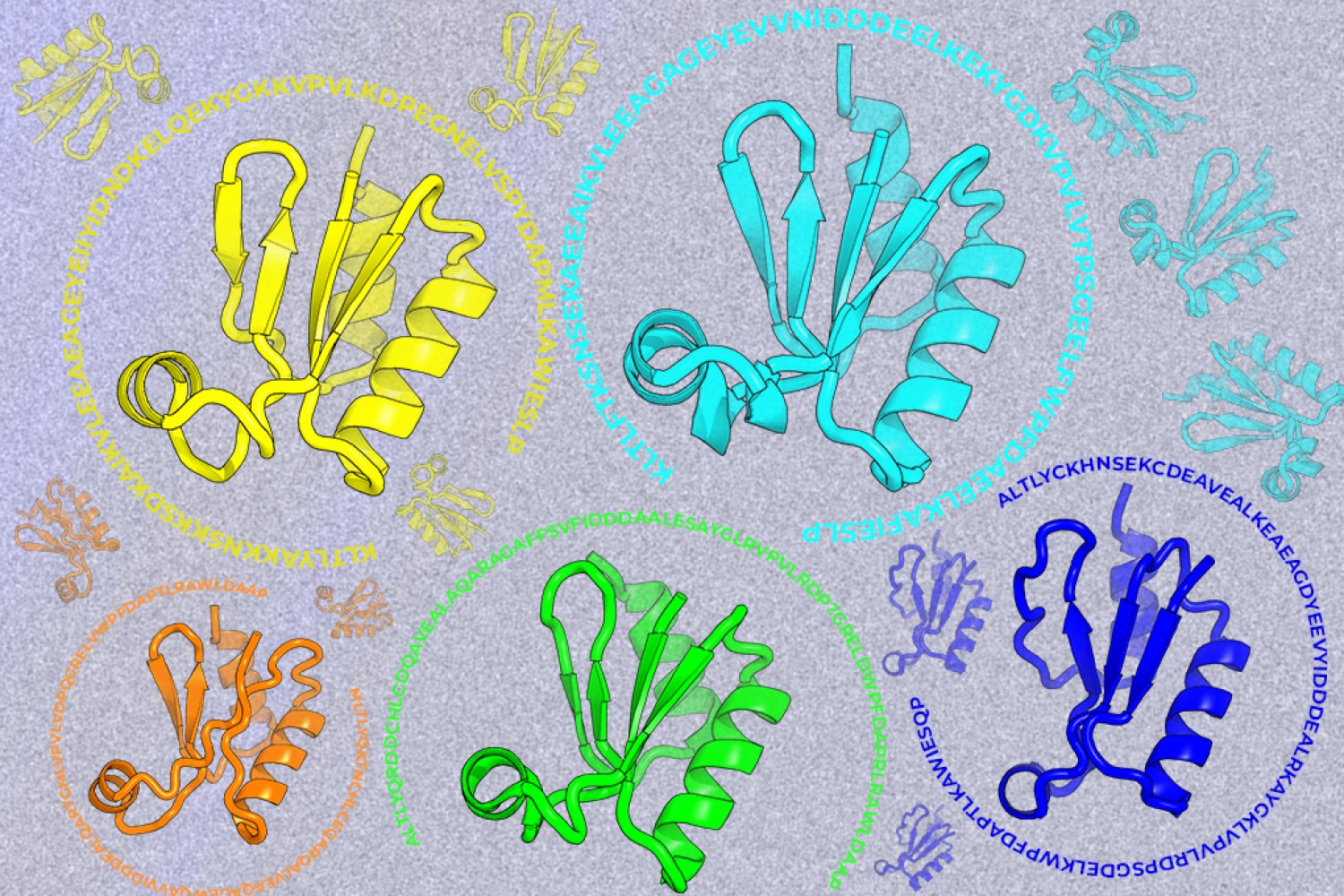
A new machine-learning framework aims to improve the success rate of computational protein design while moving away from results that reproduce sequences found in nature.